
EPISODE · Mar 18, 2026 · 20 MIN
The Photonic “Ski-Jump”: A Chip That Launches Light Into the Real World 🚀💡
from The Deep Dive Lab: Unraveling Materials Science · host Son Hoang
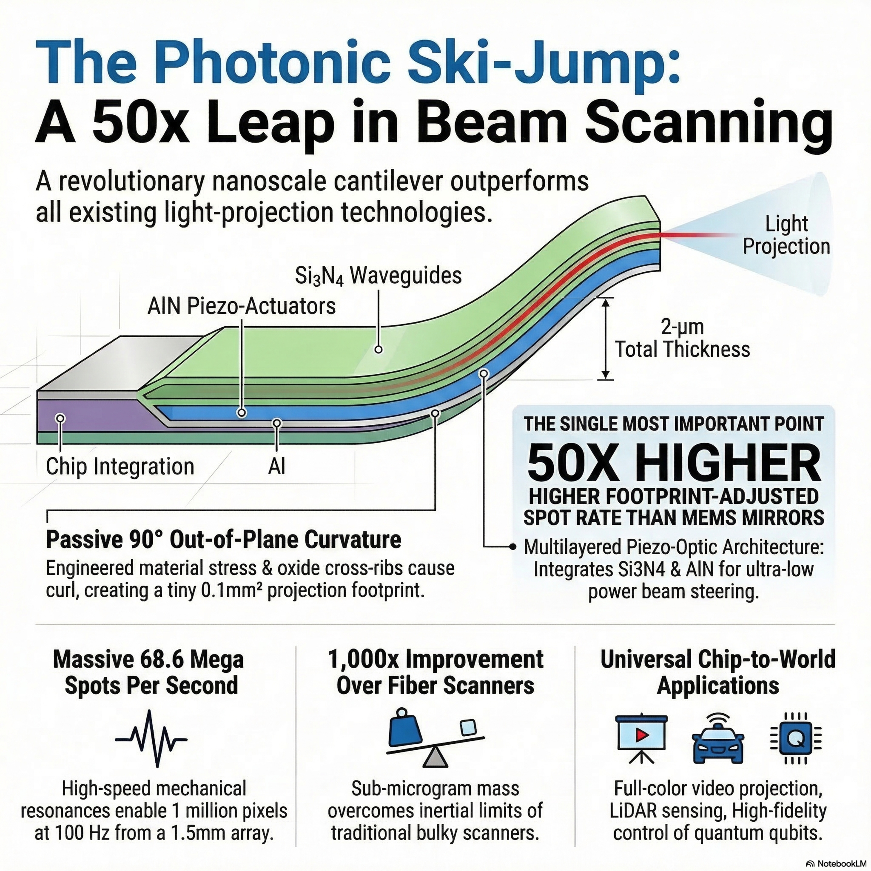
For decades, we perfected the data highways of light—fiber optics and photonic waveguides that move information across the globe at incredible speeds. But the moment light tries to leave the flat surface of a chip and enter the messy, three-dimensional world… it hits a wall.This episode explores a radical new solution: the “photonic ski-jump.” A nanoscale device that literally curls upward from the chip surface and launches light into free space with astonishing speed and precision.Engineered using piezo-opto-mechanical photonic integrated circuits (POMPIC) and fabricated with standard CMOS foundry processes, this device turns a classic semiconductor problem—thin-film stress—into an advantage. By carefully balancing layers of aluminum nitride and silicon nitride, researchers created a passive 90-degree curl that points a waveguide off-chip like a microscopic ski ramp.The result?• Beam scanning 50× faster than MEMS mirrors• 1,000× higher performance density than fiber scanners• A path to billion-pixel “Gigaspot” LiDAR engines• And even a scalable optical interface for quantum computers controlling millions of qubitsIn this episode, we unpack how a device smaller than 0.1 mm² could become the missing bridge between chips, machines, and the physical world.If a single chip can project a billion points of light per second, what happens when machines gain vision at that scale?📚 Source PaperNanophotonic waveguide chip-to-world beam scanning. Nature, Volume 651, Pages 356–363 (2026).#Photonics#Nanotechnology#IntegratedPhotonics#LiDAR#QuantumComputing#AR#Semiconductors#Optics#FutureTech#deepdivelab
Embed this episode
NOW PLAYING
The Photonic “Ski-Jump”: A Chip That Launches Light Into the Real World 🚀💡
No transcript for this episode yet
Similar Episodes
No similar episodes found.
Similar Podcasts
No similar podcasts found.