From Lab to Fab – The Atomic Leap Beyond Silicon episode artwork

EPISODE · Oct 27, 2025 · 16 MIN

From Lab to Fab – The Atomic Leap Beyond Silicon

from The Deep Dive Lab: Unraveling Materials Science · host Son Hoang

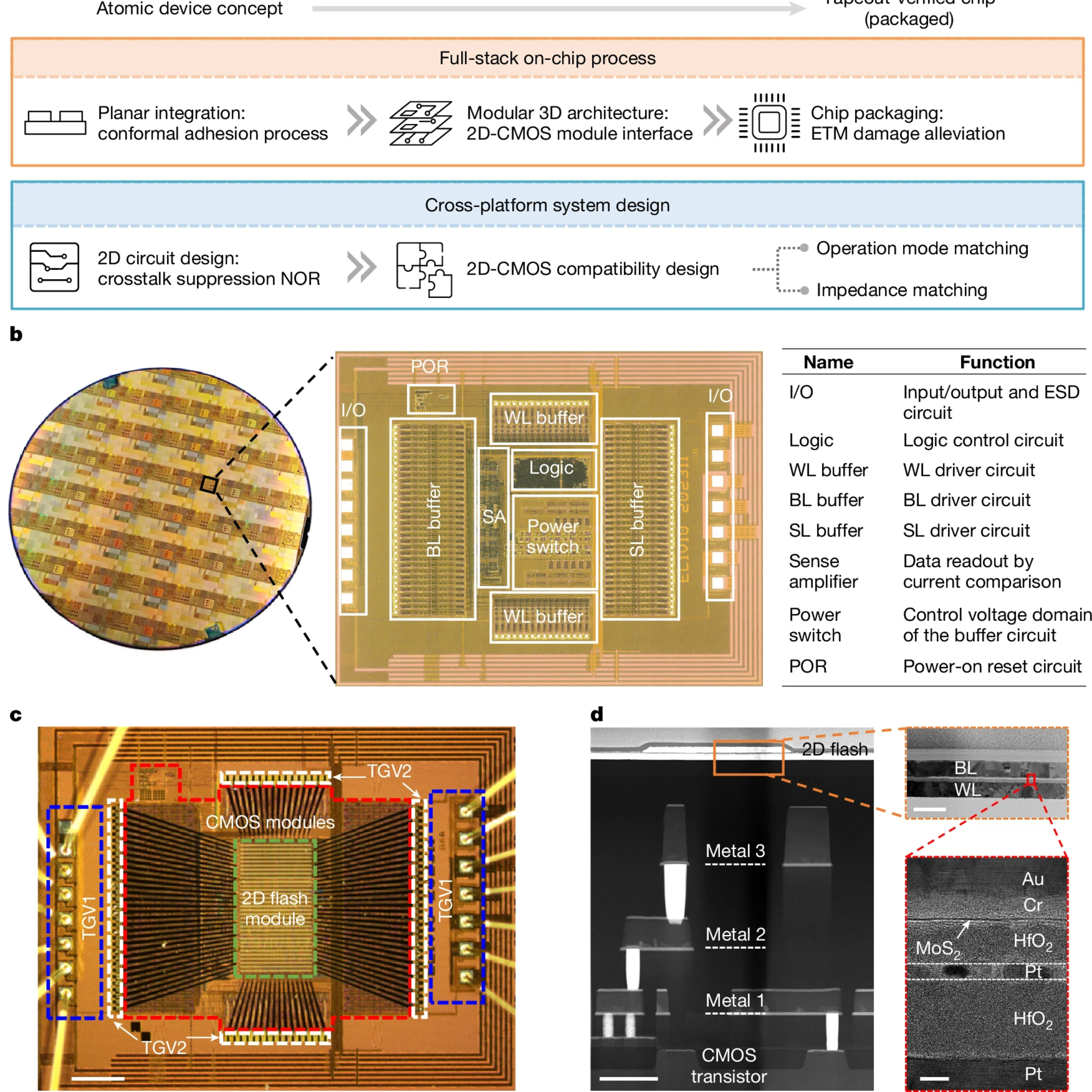
For over a decade, scientists have dreamed of building computers out of 2D materials — like 🧬 graphene and molybdenum disulfide (MoS₂) — materials so thin they’re only a single atom thick.✨ These atom-thin materials promised a revolution: faster chips ⚡, lower energy use 🔋, and computing beyond the limits of silicon.But there’s been a catch: what works beautifully in the lab often collapses in the factory.Why?Because real silicon chips aren’t smooth — they’re like a gravel road to a sheet of tissue paper. 🪶Because 2D devices speak a different electronic language from CMOS circuits. 💬And because the final packaging step — the mechanical, electrical, and thermal stress — can destroy them. 💥Now, a new framework called ATOM2CHIP has finally cracked the code 🧩 — a blueprint that teaches fragile 2D materials how to live, breathe, and work with mature silicon technology.🏗️ Through ultra-gentle adhesion, “2D-aware” circuit design, and protective packaging, researchers achieved something astonishing:✅ A fully functional 2D NOR Flash chip✅ 94.34% yield — rivaling today’s commercial silicon✅ 20 ns speed and ultra-low energy per bitThis isn’t just a new chip. It’s a new philosophy for the next era of computing — where atoms and architecture finally meet.

For over a decade, scientists have dreamed of building computers out of 2D materials — like 🧬 graphene and molybdenum disulfide (MoS₂) — materials so thin they’re only a single atom thick.✨ These atom-thin materials promised a revolution: faster chips ⚡, lower energy use 🔋, and computing beyond the limits of silicon.But there’s been a catch: what works beautifully in the lab often collapses in the factory.Why?Because real silicon chips aren’t smooth — they’re like a gravel road to a sheet of tissue paper. 🪶Because 2D devices speak a different electronic language from CMOS circuits. 💬And because the final packaging step — the mechanical, electrical, and thermal stress — can destroy them. 💥Now, a new framework called ATOM2CHIP has finally cracked the code 🧩 — a blueprint that teaches fragile 2D materials how to live, breathe, and work with mature silicon technology.🏗️ Through ultra-gentle adhesion, “2D-aware” circuit design, and protective packaging, researchers achieved something astonishing:✅ A fully functional 2D NOR Flash chip✅ 94.34% yield — rivaling today’s commercial silicon✅ 20 ns speed and ultra-low energy per bitThis isn’t just a new chip. It’s a new philosophy for the next era of computing — where atoms and architecture finally meet.

NOW PLAYING

From Lab to Fab – The Atomic Leap Beyond Silicon

0:00 16:59

No transcript for this episode yet

We transcribe on demand. Request one and we'll notify you when it's ready — usually under 10 minutes.

No similar episodes found.

No similar podcasts found.

Frequently Asked Questions

How long is this episode of The Deep Dive Lab: Unraveling Materials Science?

This episode is 16 minutes long.

When was this The Deep Dive Lab: Unraveling Materials Science episode published?

This episode was published on October 27, 2025.

What is this episode about?

For over a decade, scientists have dreamed of building computers out of 2D materials — like 🧬 graphene and molybdenum disulfide (MoS₂) — materials so thin they’re only a single atom thick.✨ These atom-thin materials promised a revolution: faster...

Can I download this The Deep Dive Lab: Unraveling Materials Science episode?

Yes, you can download this episode by clicking the download button on the episode player, or subscribe to the podcast in your preferred podcast app for automatic downloads.
URL copied to clipboard!